Dumping an external EEPROM
October 17, 2018
Part I: I2C/TWI EEPROM
I’m going to use the Arduino Wire library to communicate with the EEPROM over I2C. On the UNO, SDA is A4 and SCL is A5. You can see pinouts for other boards on the Wire Library reference page. This page shows more details about how the Wire library works.
Fortunately this chip has legs that are spaced out enough for my cheap logic probes. I setup my scope to eavesdrop on the SDA and SCL lines so that I could verify the code was operating as desired. This also allowed me to determine that the clock frequency being used in the original circuit was about 30 kHz.
#include <Wire.h>
#include <stdint.h>

#define AT24C02_ADDR 0x50

void setup() {
  uint8_t dataAddr;
  Serial.begin(9600);
  Wire.begin();
  Wire.setClock(31000L); //31 kHz
  Wire.beginTransmission(AT24C02_ADDR);
  Wire.write(0x00); //Sets the start address for use in the upcoming reads
  Wire.endTransmission();
  for(uint8_t i=0;i<8;++i){ //cycle through enough times to capture entire EEPROM
    Wire.requestFrom(AT24C02_ADDR,32,1); //read 32 bytes at a time
    while (Wire.available()){
      uint8_t c = Wire.read();
      Serial.write(c); //Send raw data over serial to computer
    }
  }

}

void loop() {

}
I recommend viewing the output in RealTerm. Shown below are the settings I used to connect, your port will probably be different.
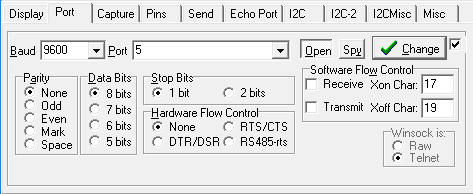
Once connected, I reset the UNO and told realterm to display the data coming over the serial connection as hex values.
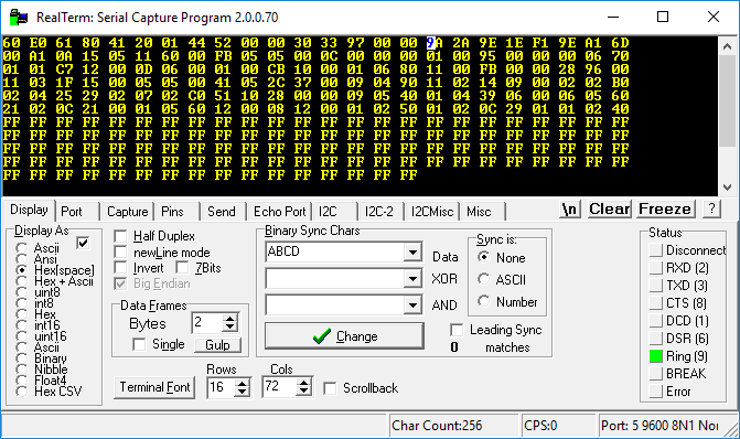
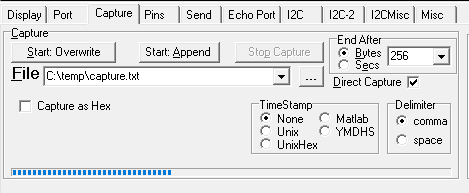
Once I could tell it was working, I had realterm capture the output to a file.
Binary file of EEPROM contents. This EEPROM is from a Genesis Resource dive computer (link to teardown post). Now that you have the file you can use a variety of utilities to examine the data.
For example, hexdump:
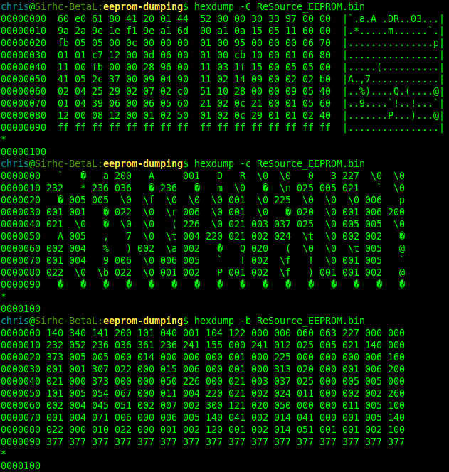
See this page for helpful info on using hexdump.
Part II: SPI EEPROM
- Datasheet for the AT25256 EEPROM
- Code used on the UNO (also shown below)
#include <stdint.h>
#include <SPI.h>

const uint8_t chipSelectPin = 10;
const uint8_t RDSR = 0x05; //Read Status Register
const uint8_t READ = 0x03; //Read command, to be followed by 16 bit address
uint16_t readAddr = 0x0000;// Address to start reading at
uint8_t outputByte = 0;

void setup() {
  Serial.begin(115200);
  SPI.begin();
  pinMode(chipSelectPin, OUTPUT);

  //Sets up the parameters for SPI communication
  //800 kHz clock, big-endian (most significant bit first),
  //mode 3 (clock default is high, data read on rising edge)
  SPI.beginTransaction(SPISettings(800000, MSBFIRST, SPI_MODE3));
  delay(10); //probably not really needed

  digitalWrite(chipSelectPin,LOW); //Activate EEPROM
  SPI.transfer(READ);
  SPI.transfer16(readAddr);
  for(uint16_t i=0;i<32000;++i){//This EEPROM has 256kbits / 8 = 32kBytes
    outputByte = SPI.transfer(0x00);
    Serial.write(outputByte); //Sent raw binary data over serial
  }

  digitalWrite(chipSelectPin, HIGH);
  SPI.endTransaction();


}

void loop() {
}
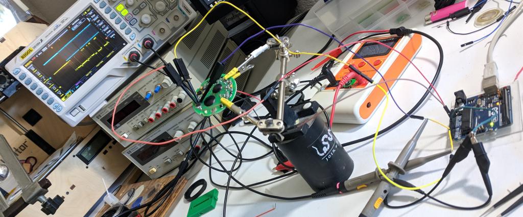
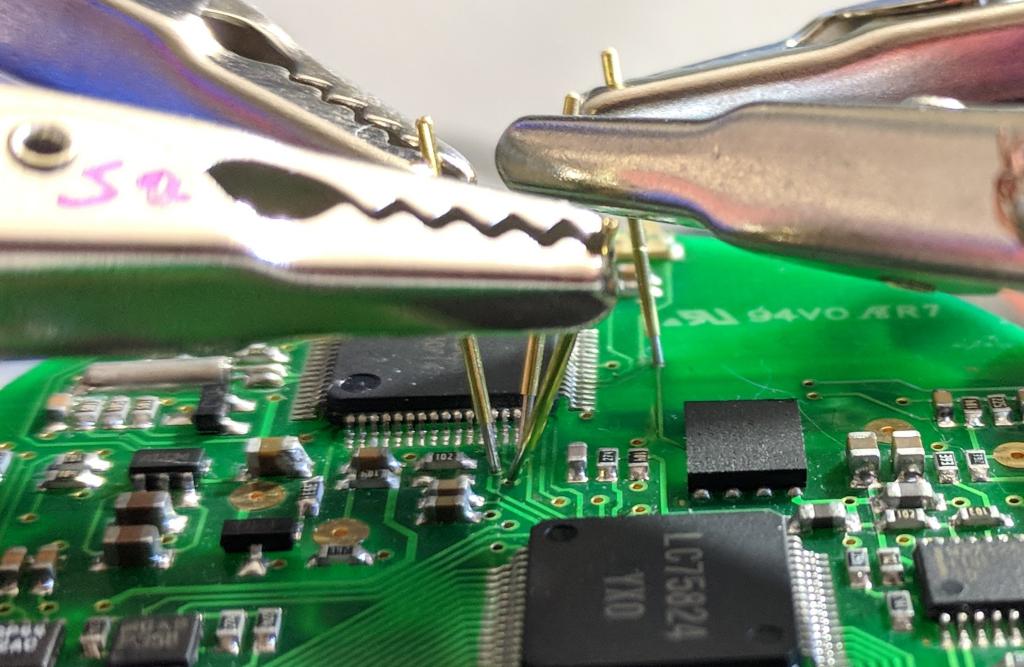
Since my logic probes aren’t small enough to attach to the legs of the surface mount components on this PCB, I rigged up a different solution using coolant hoses, alligator clips and pogo pins.
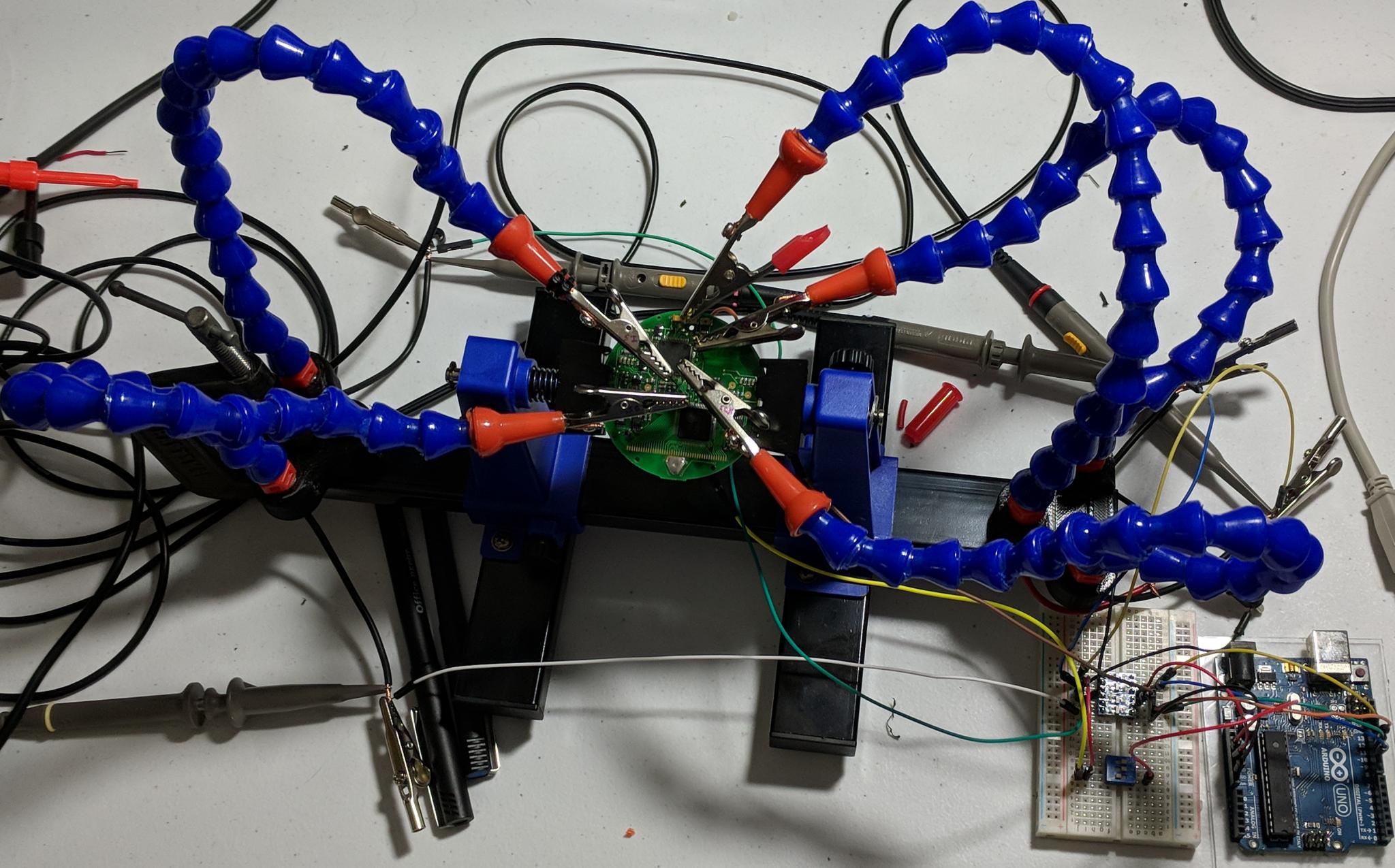
It actually worked quite well.
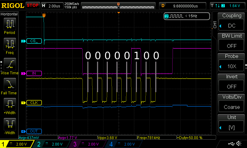
Before connecting the UNO I sniffed the boot up communications between the onboard MSP430 and the EEPROM. The first communication on each power on is shown below. Looking at the data sheet (page 6) we can see that is the WRDI (Reset Write Enable Latch) command, also known as the Write Disable command. The datasheet says it boots with write disabled so I guess this is just to be extra cautious about preventing accidental writes?
The READ command format is 0000.X011 (where the X means that could be either 0 or 1 and has no effect). In HEX this is 0x03 (assuming a 0 for the don’t care bit). To read back the memory contents starting at a specific address, the master must send this command followed by the 16bit address. Once those three bytes have been sent to the slave, the slave will respond with the byte at that memory address the next time the master sends a byte. The slave will then automatically increment its internal address counter so that to keep receiving data all the master has to do is keep sending dummy bytes.
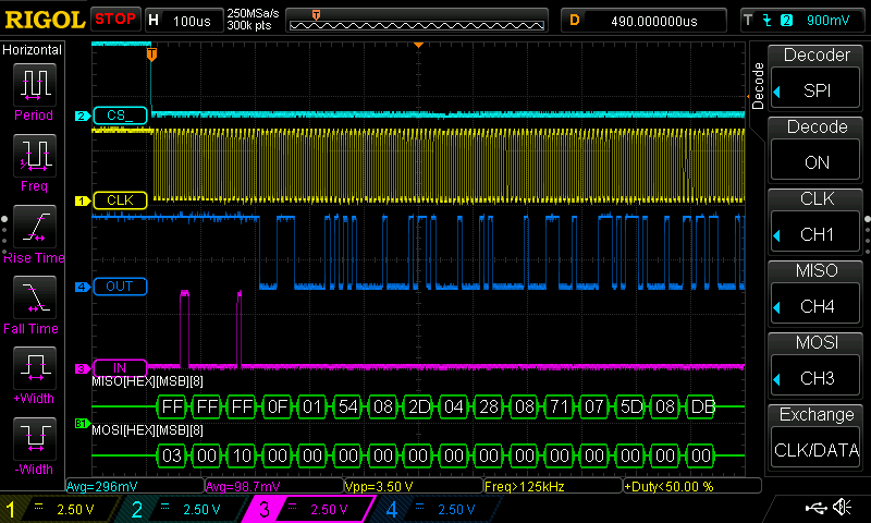
Below you can see a READ starting at address 0x0010. This is the memory location accessed by the onboard MSP430 shortly after boot-up. Sniffing this before manually accessing the EEPROM meant I could compare against it later to be sure my dump was correct.
At the bottom of the screenshot you can see that the scope is automatically decoding the bits. The MOSI (Master Out Slave In) corresponds to the purple (IN) trace. The first byte is the READ command followed by the address 0x0010. Then jumping up tot he MISO (Master In Slave Out) line you can see the data being returned.
Before hooking up the UNO, I used a fifth pogo pin to connect to the reset pin on the MSP430. Holding this pin low keeps the microcontroller in reset which means the pins connected to the EEPROM will be tri-stated (high impedance). This is important so I don’t have the MSP430 trying to hold a pin low while the UNO tries to hold it high (or visa versa) causing a short circuit. I checked that the pins were actually tri-stated by hooking up a 10k pull-up to each pin being pulled low. Since the 10k pulled the voltage immediately up to Vcc, the pin had to be high impedance.
The Chip Select line I connected to digital pin 10 on the UNO. The clock line is connected to pin 13, MISO to pin 12 and MOSI to pin 11. Since this EEPROM runs at 3.3 volts and the UNO uses 5 volts, I connected everything through a logic level shifter and used the 3.3 volt rail from the UNO to power the EEPROM.
The actual dumping process is nearly identical to that shown above (use RealTerm except set the baud rate to 115200).
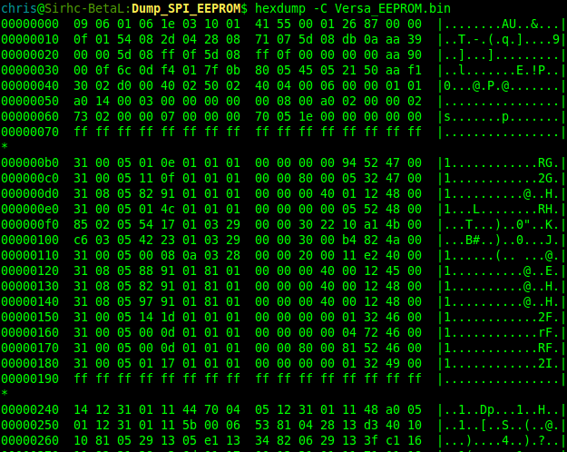
Binary file of EEPROM contents. This EEPROM is from an Oceanic Versa Pro dive computer (link to the teardown post). Shown below is the first section, formatted using hexdump.