
Reverse Engineering an LCD dot-matrix display
January 12, 2018
A few months ago I popped into Goodwill to see if they had any interesting electronics to take apart. I was rewarded with a fully functioning 1993 Smith Corona electric word processor for all of $5. After playing around with it for a few days and learning how it worked, I took it apart and turned it into a box of interesting electrical and mechanical doodads.
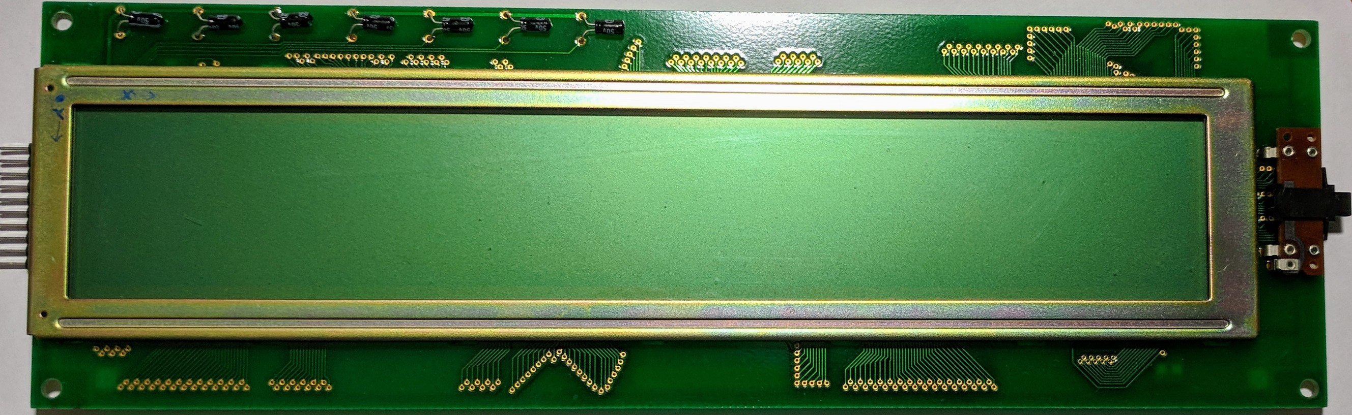
One of the components was a 480x64 pixel dot-matrix style LCD display (LMG6721UHGR) which I decided to use for a project. I already had a few of the 16x2 character LCDs and a Nokia cell phone screen breakout board I could have used, but those are pretty small and I was intrigued by the idea of reusing this old display.
The Hardware
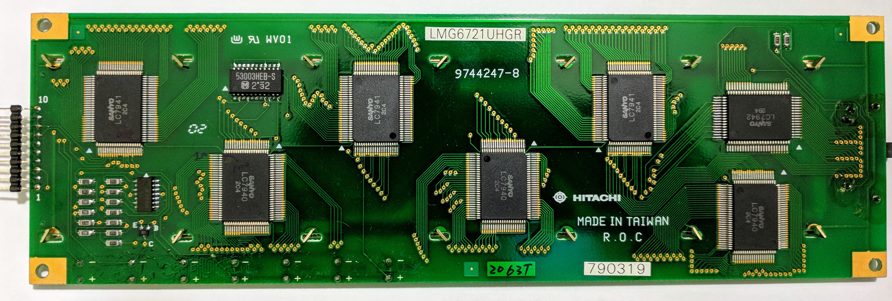
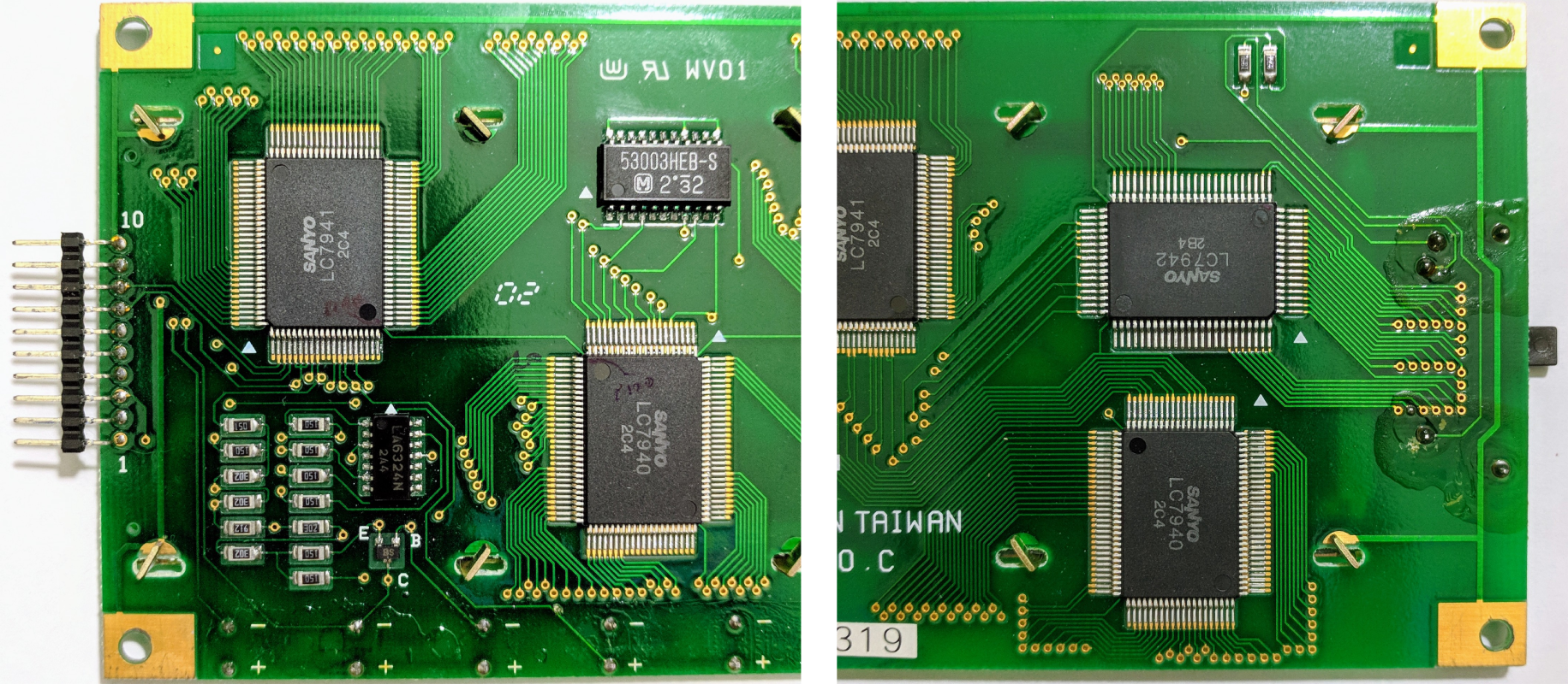
The circuit board the screen is attached to has a ten pin row of standard 0.1” headers which provided the connections back to the main control board when it was in the typewriter. The circuit board has seven large ICs and two smaller ICs. After googling for the datasheets it turns out that one of the smaller ICs is a quad opamp (LA6324N) which provides the required voltages for driving the LCD cells (more on that later). The other small IC (53003HEB-S) is some sort of counter (I haven’t been able to find a datasheet for it). Six of the large ICs (three LC7940 and three LC7941) control the 480 columns (80 columns for each chip). The seventh (LC7942) controls the 64 rows.
Datasheets
My next task was to determine which signals are broken out to the header pins and how the LC794x ICs work. After a few hours of referring to data sheets, learning how LCDs work, and many continuity measurements I determined the pinout for the headers and what pins on the driver ICs are connected to what.
 The headers are shown as viewed in the picture of the back of the screen (above). The labels are referring to the pins on the driver ICs.
Each column of pixels is controlled by the six 7940 and 7941 ICs, the pinout for which is shown below.
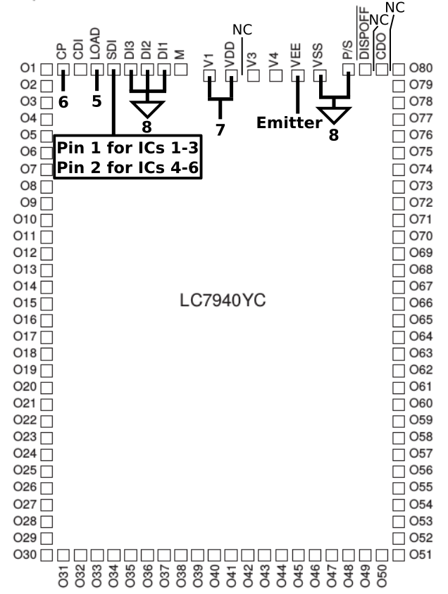
The 7940 and 7941 are the same IC, just with their pins flipped to help with dense circuit designs. The figure above matches the lower three ICs in orientation, but since the pins are flipped on the upper three ICs the order of the pins ends up being the same. The numbers refer to the pin number in the headers pins. (I’ve noted where physical pins exist but aren’t shown in the pinout diagram because they don’t connect to anything internally.)
The P/S pin is pulled low which sets the IC to serial data input mode. The pins which would be used for parallel input (DI1,2,3) are also pulled low. The screen is split into a left half and a right half. The three ICs controlling the left half get data from header pin 1 and the three ICs controlling the right half get data from header pin 2. Strangely the DISPOFF pin doesn’t seemed to be pulled up or down.
CDI on the first IC of each set of three is pulled low. The CDO pin of the first IC is connected to the CDI pin of the second, and the CDO of the second connected to the CDI of the third. The CDO of the third IC in each set isn’t connected to anything.
The rows are controlled from the LC7940 driver IC which is shown below rotated by 180 degrees to match the orientation in the picture of the back of the screen (above). See the datasheet for the regular orientation.
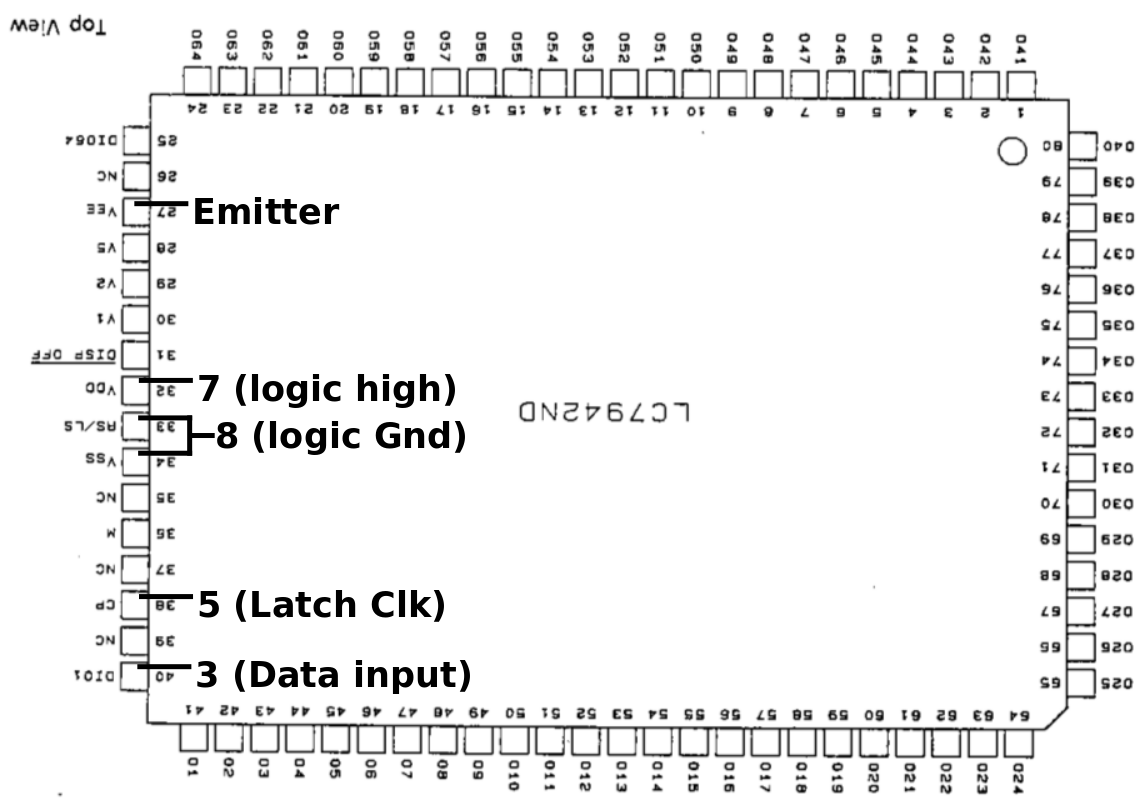
The RS/LS pin is pulled to logic low which sets the shift direction to “right shift”, meaning DIO1 is the input, DIO64 is the output, and the data shifts from O1 to O64. This chip behaves exactly like a shift register, so data shifted into DIOI on the falling edge of the first clock pulse is shifted out of DIO64 at the 64th falling edge. This allows chaining to control displays with more than 64 columns. In this display O1 is connected to the top row and O64 is connected to the bottom row.
Driving an LCD
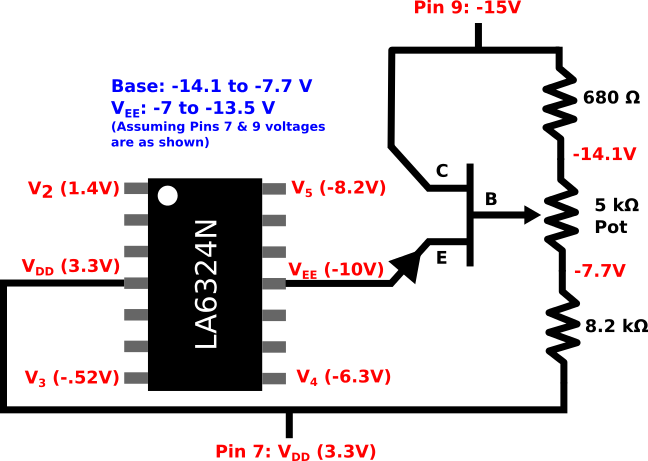
The driver ICs utilize seven different voltage levels. Three are from header pins 7, 8 and, via the transistor, pin 9. The remaining 4 are created by the quad opamp IC.
In order from highest to lowest:
VDD = V1 (logic high), V2, V3, V4, V5, VEE (LCD Gnd)
Shown below are how V2 through V5 relate to VDD and VEE along with example numbers assuming VDD=3.3V and VEE=-10V.
Let |dV| = |VDD - VEE|.
- V2 = |dV|*(6⁄7) - |VEE| = 1.4V
- V3 = |dV|*(5⁄7) - |VEE| = -0.52V
- V4 = |dV|*(2⁄7) - |VEE| = -6.3V
- V5 = |dV|*(1⁄7) - |VEE| = -8.2V
Logic low (Vss) will be close to V3, but could be above or below it depending on the what the pot is set to (since the pot controls VEE).
The image below shows how the voltage generation circuitry using 3.3 volts as logic high and with -15 volts connected to pin 9. The voltages are all measured relative to logic low. The potentiometer adjusts the voltage difference between the collector and the emitter which changes VEE. The end effect of this is to change the screen contrast.
To understand why all the voltages are required (and what the yet to be mentioned “M signal” does), we have to delve into the workings of Liquid Crystal Display technology.
A common LCD panel configuration consists of two polarizers at right angles to each other sandwiching the cell structure containing the “liquid crystal” as well as sheets of transparent electrodes on each side of the liquid crystal sheet. Light passing through one polarizer is then rotated 90 degrees by the liquid crystal such that it lines up with the second polarizer. Thus the default state is a “clear” pixel. When a voltage is applied to the electrodes, the crystal structure is untwisted meaning the polarization angle of the light is no longer being rotated and so will be perpendicular to the second polarizer causing the light to be blocked and the pixel to turn black.
Unfortunately, things get a bit more complicated. If you apply a DC voltage to a cell it will work but not for long. The crystal structure will degrade and the electrodes will cease to be transparent. The solution is to apply an AC voltage centered on zero. The voltage across the cell can’t simply go from say 10 volts to 0 and back to 10, it must flip polarity each cycle. So if one moment electrode A is 10 volts higher than electrode B, the next moment electrode A must be 10 volts lower than electrode B. Not only does this switching need to occur when the cell is activated, but also when in it’s inactive state.
See these wikipedia pages for more info: Effect of Chirality and Twisted nematic field effect
The total voltage difference across a cell is determined by the difference between the voltages output by the column drivers and the row driver. For the column drivers, selected (dark pixel) voltages are V1(VDD) and VEE and not-selected (clear pixel) voltages are V3 and V4. For the row driver the selected voltages are the same, but the not-selected voltages and V2 and V5.
Which voltage is output at any given moment is a function of the M level and the Q level (corresponding to the electrode being ON or OFF).
| Q State | M | Row | Col | Row-Col |
|---|---|---|---|---|
| ON | Low | VDD | VEE | +13.3 |
| ON | High | VEE | VDD | -13.3 |
| OFF | Low | V2 | V3 | +1.9 |
| OFF | High | V5 | V4 | -1.9 |
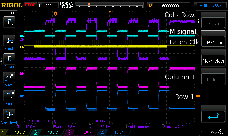
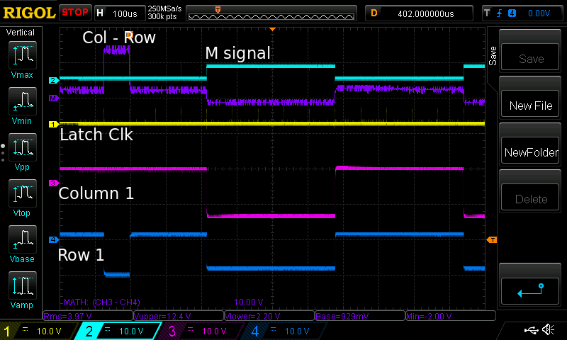
For a pixel to be OFF (clear) the voltage difference between the electrodes is 1.9 volts and for a pixel to be ON (dark) the voltage difference is 13.3 volts. The scope output below shows the voltages on the electrodes for row 1 and column 1, as well as the latch/load clock and the M signal for one complete frame. The M signal alternates every 5 falling edges of the load/latch clock (look for the very thin yellow peaks) and the electrode voltages swap each time the M signal changes. This output shows the somewhat unrealistic, but helpfully illustrative, case where every row and every column are ON at all times. Normally only one output of the row driver IC would be activated at any given moment.
The MATH output shows the column voltage minus the row voltage. This alternation results in a AC signal with a peak-to-peak amplitude of 2*|VDD-VEE|.
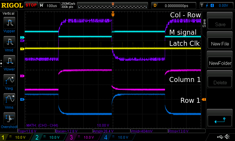
The following scope output shows exactly the same signals, just zoomed in on the time axis.
The next output still shows the same signals, but with the more realistic scenario where the rows are being activated one at a time while every pixel in every column is ON (dark). Each row is being turned dark one at a time as the row IC driver shifts through it’s 64 outputs before starting again.
Looking at the results of the difference between the row and column voltages, it is clear that the difference in voltage is large enough to darken the pixels in row 1 only for the time between the first and second latch clock pulses. Since the M signal changes every 5 latch clocks and that doesn’t divide evenly into 64, the voltage applied to the cells in this row will keep flipping as the row driver IC loops back around.
Loading Data
In brief:
- The output buffer of each column driver is serially filled with 80 bits of data
- Each bit gets read in on the falling edge of the data clock
- Once the buffer is full the first time, the latch clock latches the buffer out to the drive circuitry
- At effectively the same moment the frame clock shifts a 1 into the first bit of the row driver
- The column buffers get refilled (240 data clocks), the active output of the row driver shifts to the next row and the column data is latched to the pins.
- This continues over and over with a 1 getting shifted into the row driver every 64 latch clocks
Filling the Column Buffers
The screen is split into two sections, each 240 pixels wide. The two halves are loaded in parallel and all the logic is the same for each half. Until I get into the software we can ignore the right half of the screen and pretend there are only three column driver ICs.
All three ICs have their serial inputs connected together and brought out to header pin 1. This means each IC sees all 240 bits of data but only accepts 80. This is accomplished though the CDI and CDO pins. When CDI (Chip Disable) is low the chip is enabled and will read in data from the serial input. When the CDI pin is high it won’t. The following steps go through the process of filling all three buffers.
- Start with all buffers empty (due to the latch clock)
- CDI1 is held low, CDO1/CDI2 and CDO2/CDI3 begin high
- After the first 80 bits have been read into IC1, CDO1 (and thus CDI2) goes low
- IC1 is full and so will ignore the remaining 160 bits
- The middle set of 80 bits are read into IC2, CDO2/CDI3 goes low
- IC1 and IC2 are both full and thus ignore the remaining 80 bits
- The last 80 bits are read into IC3
The scope output below illustrates these steps. CDI1 is not shown since that pin is always held low. CDO1/CDI2 is high for the first third of the data and CDO2/CDI3 is high for the first two thirds.
Multiplexing
There are three “clock” signals which control the ability to multiplex the data, thus controlling many pixels with only a few pins.
- The Data Clock (CP) controls the loading of data into the buffers in the column driver ICs, the state of the SDI pin is read in on each falling edge of the data clock.
- The Latch Clock (load) has several roles
- It controls when the column buffers are latched to the output pins
- It provides the clock signal to the counter IC which produces the alternating M signal every 5 latch clocks
- It provides the clock signal to the column driver, shifting the active row each time.
- The Frame Clock (DIO1) is really the input data signal for the row driver IC, the state of which is clocked in by the latch clock. However, it’s useful to think of it as the “clock signal” which begins a single frame.
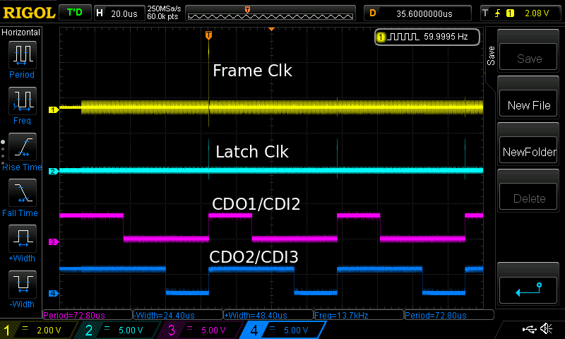
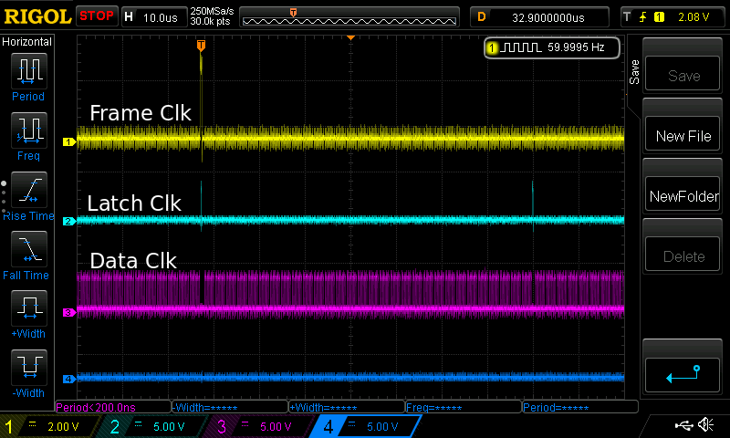
The following scope output shows the relationship between the data clock, latch clock and frame clock. There are 30 groups of 8 data clock pulses between each latch clock due to the data being read in one bit at a time from 8 bit chunks.
Real Example
The scope output below shows the beginning of a row where the data 01110 is being loaded, corresponding to three dark pixels with a clear pixel on either side.
![]()
Read Part Two!