Building an inverting charge pump
January 20, 2018
I’ve been using a bench power supply to provide the required negative voltage supply for the LCD screen I reverse engineered. I want to make this project portable, so everything needs to run off a USB battery pack. These tend to be lacking in “non-5V” power rails, so I built an inverting voltage charge pump.
The LCD display is composed of many cells forming pixels and each cell behaves very much like a capacitor. This means that there is very little net flow of current. Hooking up a multimeter showed that I really only need to provide a voltage rail at -13.5 volts, or lower, capable of approximately 3 mA. A charge pump is a cheap easy solution when dealing with currents lower than a few tens of mA. The main benefit of a charge pump is that it only uses diodes and capacitors combined with a square wave to generate the output voltage. No comparatively expensive or bulky inductors are required.
Dave Jones has done a few great videos on the EEVBlog explaining both inverting and non-inverting charge pumps, so for an explanation of how they work check out the following links.
- EEVblog #469 - Cockcroft-Walton Multiplier
- EEVBlog #473 - Microcontroller Voltage Doubler
- EEVblog #483 - Microcontroller Voltage Inverter Tutorial
The image below shows a five stage inverting voltage multiplier. The ideal voltage outputs are labeled at the bottom of the diagram. The last stage gives -5*Vin = -25 volts. Of course in the real world there are diode drops and output impedance to deal with. In practice I was able to achieve a no-load output voltage of around -21 volts.
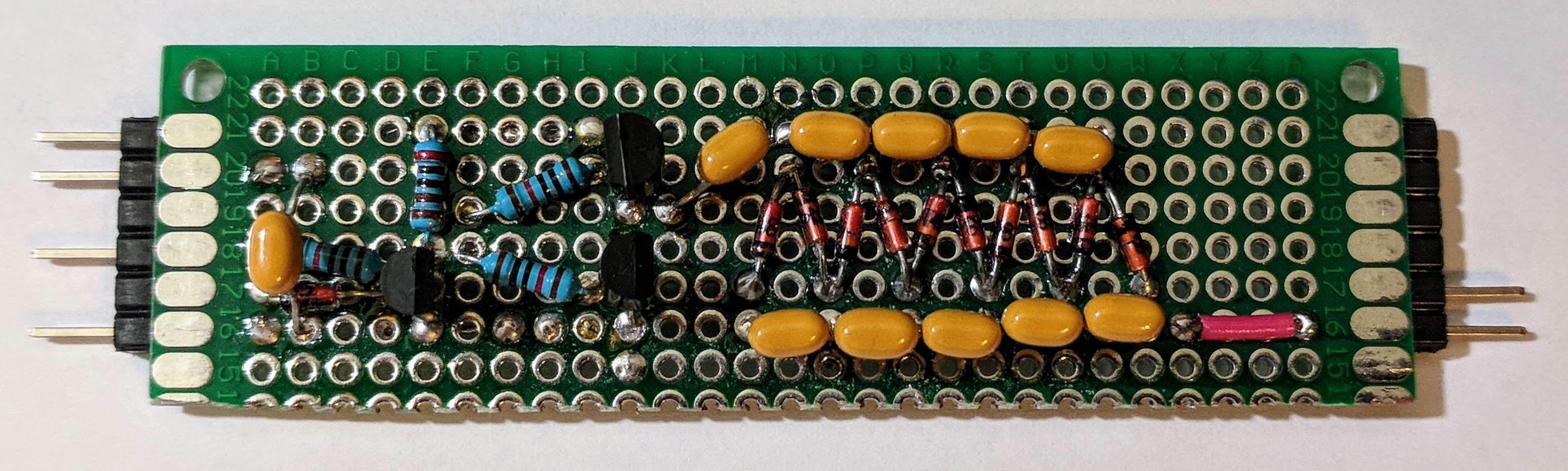
Starting on the left side of the circuit, there is a logic level shifter followed by a push pull amplifier and then the five “pump” stages.

Let’s go over the circuit in a bit more detail.
- Capacitor C11 provides smoothing for the input voltage and helps prevent noise from getting back to the microcontroller.
- Transistor Q2 combined with resistors R1, R4, and diode D11 shift the 3.3 volt square wave coming from the micro to a 5 volt square wave needed to drive the push-pull amplifier stage. See the end of this post for more details on this stage (such as what the diode is doing).
- Transistors Q1 and Q3 with resistors R1 and R2 form the push-pull amplifier. This takes the fairly high output impedance 5 volt square wave coming from the logic level shifting stage and creates a very low output impedance square wave. Q1 slams the voltage down to ground and Q3 slams the voltage up to 5 volts. Pulling more current won’t significantly impact the peak to peak voltage of the square wave which means the pump stages will get a nice constant input.
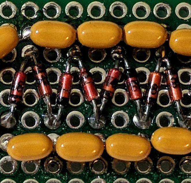
- Each charge pump stage consists of two capacitors and two diodes. Ideally these would be Schottky diodes to reduce the losses due to the forward voltage drop, but I only had one Schottky diode and a whole bag of 1N4148 diodes. I tried both 1uF and 10uF ceramic capacitors and found the 10uF caps worked better.
I constructed the circuit on a proto board laid out nearly exactly as shown in the diagram. On the left, the lowest pin is GND, the next is the PWM input and the top two pins are both Vin = 5 V. On the right, both pins are the negative voltage rail output.
The screen capture below shows the unloaded output voltage and the PWM signal. The output signal is AC coupled so that the noise can be observed. When unloaded there is no noticeable ripple, but there is the switching noise associated with the rising and falling edges of the square wave.
A multimeter reading shows -21 volts.

The next screen capture shows the waveform when the output is connected to a resistor drawing 3.3 mA. Once again the switching noise is evident, but now the ripple dominates. Peak to peak ripple (not accounting for switching noise) is ~100 mV.
A multimeter reading shows -14 volts.

Appendix
When testing the voltage level shifter portion of the circuit I encountered an interesting issue. At low frequencies the turn on and turn off times of the transistor can be neglected, but at high frequencies the turn off time becomes a significant percentage of the PWM period.
In the screen capture below (and all the following captures) the yellow signal is the PWM output measured directly from the uC pin, the light blue signal is the voltage on the base of the transistor, and the dark blue is the collector voltage. The shifter both shifts the high voltage from 3.3 to 5 volts and inverts the output (in a logical “NOT” sense). The transistor turns off when the PWM signal goes low, at which point the 2 kOhm resistor pulls the collector voltage high. The transistor turns on when the PWM signal goes low, pulling the collector voltage to ground.
The transistor turns on very quickly (less than 100ns), but it takes around 1.5 us for it to turn off after the PWM signal goes low. At a PWM frequency of 80 kHz, this is about 12% of the period. What this means is that if I set the PWM frequency to a +duty cycle of 50%, the +duty cycle of the level shifter will be about 40%. I could fix this in software by setting the +duty cycle to 60%, but I’d prefer to fix it in hardware.

The root cause is that when the transistor is in saturation (fully on, collector voltage low), it takes a while to remove enough charge carriers to turn it off.
Below I show two possible solutions. Both involve adding a component in parallel with the base resistor which allows charge carries to be removed more quickly.
Solution One
The first solution is to place a capacitor in parallel with the base resistor. The rising and falling edges of the square wave are composed of very high frequency components to which the capacitor appears as a very low impedance path. This does make the turn on and turn off times of the transistor extremely fast, but it makes the base voltage go down to -3.3 volts for half of each cycle. From what I read, this will eventually make the transistor degrade.

Solution Two
The other solution is to place a diode in parallel with the base transistor (with the low side away from the transistor). When the PWM signal is high, the diode is reversed biased thus effectively not a part of the circuit. But when the PWM signal is low, the diode is forward biased and allows the charge carriers to leave the transistor much faster.
The following plots show the results for a variety of diode types.
The first diode is the 1N4148 which does improve the turn off time, but not as much as I would like. This is due to the forward voltage of the 1N4148 being basically the same as the transistor PN junction forward voltage.

The next is a 1N4001, which although the diode takes a longer time to fully turn on (as it’s not a high speed switching diode like the 1N4148), it turns on more in the initial few ns. With this diode, the turn off time is quite good though there is a decent amount of ringing when it turns back on.

The generally recommended diode is a Schottky diode due to its low forward voltage. The next screen capture shows a 1N5818 Schottky diode which results in an extremely short turn off time, but a great deal of ringing. Measuring the capacitance of this diode we can see that it is around 150 pF.

The diode I went with is the 1N60 germanium diode. This diode has a very low forward voltage drop but the capacitance is only around 15 pF. The result, shown below, is a very fast turn off time but no ringing.
